источники информации:
http://www.phyton.ru/support/nand-flash-structure
http://www.stlinux.com/howto/NAND/BadBlocks
Data storage on NAND Flash
Single Level Cell (SLC) NAND Flash stores one single bit of information for each memory cell. This is the only type of NAND technology that the STMicroelectronics’ drivers can support. There are other NAND technologies, such as Multiple Level Cell (MLC) which stores multiple bits of information for each memory cell and so provides higher storage density. However, MLC NAND Flash is slower, less robust and consequently requires a more sophisticated error correction mechanism. A third technology, Triple Level Cell (TLC), is also available, but this demonstrates the same disadvantages as MLC.
The basic unit of operation for a NAND Flash device is the page. Generally, the page is the smallest writable unit of the NAND device. A block consists of a multiple number of pages, and is the smallest erasable unit of a NAND device. There are certain NAND Flash commands that can be applied to a given page, others that are applied to a given block, and some that can only be applied to the whole chip.
Before programming, a page is erased by setting all data bits to «1». The controller writes data to the page by setting selected cells in the page to «0». This means that the data is effectively recorded in the page by applying a logical AND to the existing state of the chip; bits at «1» can be programmed to «0», but bits at «0» can only be changed to «1» by erasing the entire block.
Every page is divided into two distinct regions, the In-Band area and the Out-Of-Band area (OOB). Both areas are freely addressable by the user. Under normal usage, the In-Band area is for main data storage and the OOB area is for Error Correcting Code (ECC) and metadata. However, there is no underlying difference between the In-Band and OOB cells and other layout strategies exist, such as interleaving data and ECC sectors, treating the Page and OOB area as a single unified entity.
NAND Flash devices can be characterized by the size of the pages. As the page is the smallest addressable unit of a Flash device, then a page size should be chosen that enables the memory to be used efficiently.
The following table gives details of the four most common page sizes, and the size of the In-Band and Out-of-Band areas for each.
| In-Band area | Out-of-Band area | |
|---|---|---|
| Small page | 512 bytes | 16 bytes |
| Large page | 2048 bytes | 64 bytes |
| Very large page | 4096 bytes | 128 bytes |
| Very very large page | 8192 bytes | 256 bytes |
Note that the command protocols for the different page sizes are different, so components that need to access NAND must be configured according to the size of the page in use.
Out-of-band (OOB) area
The OOB is traditionally 1/32 of the size of the In-Band area, although some modern NANDs require a larger OOB. It is used for Error Correcting Code (ECC) and metadata. The following list describes some of the metadata that can be found in the OOB:
- manufacturer’s bad block markers
- filesystem metadata (for JFFS2, YAFFS, and others)
- the BBT «magic signature»
- ST’s own special tags
In some cases, the ECC scheme is such that there is little or no free space in the OOB area for storing the required metadata. Hardware constraints may impose further restrictions on the use of the OOB area. Consequently, it is not always possible to support all users of the OOB area, or in other cases, support needs to be adapted accordingly (for example, moving the BBT signature in-band, or invoking the YAFFS2 ‘inband-tags’ option).
Large block vs. Small Block NAND
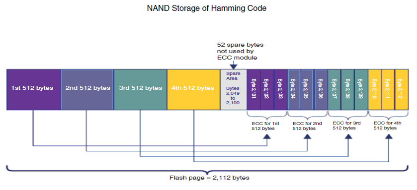
In the current NAND architecture, each page consists of 528 bytes, and each block consists of
32 pages. Future NAND devices will use the large page/large block structure in which a page will
be 2112 bytes (4 times larger) and a block will consist of 64 pages (2 times larger) resulting in a
block size that is 8 times larger. The first of these new large block NAND flash devices is the 1
Gbit TC58NVG0S3AFT00. Note that all large block devices will also have the chip enable don’t
care feature. The increased page and block size will enable faster program and erase speeds in
future high density NAND flash.
ECC